Introduction
The Esaki tunnel diode is a semiconductor p-n junction that uses the phenomenon of quantum tunneling to its advantage. The junction between the two doped semiconductor materials creates a potential barrier between the valence band of the p-type material and the conduction band of the n-type material. If the potential barrier is thin enough, and depending on the bias of the junction, individual electrons can tunnel either “forward” or “backward” through the potential barrier, collectively creating a current. In fact, the tunnel diode exhibits the unique characteristic of having negative resistance at particular levels of forward bias. I have approximated this potential barrier in order to perform the sort of one-dimensional analysis we did in class. My goal is not to find accurate numerical quantities that describe a real-life Esaki diode, but rather to apply what we learned about potential barriers in class in order to demonstrate the relationship between the dimensions of a barrier and the transmission coefficient of an incident wavefunction in the context of a real device.
Background
Whereas electrons in individual atoms have discrete, quantized energy levels, electron in solids interact with each other in such a way as to form continuous “bands” of allowed energy. In semiconductors, we focus on the valence and conduction bands. At absolute zero, the states in the valence band are full, but optical or thermal excitation can excite electrons up to the conduction band – a necessary condition for the semiconductor to conduct electricity. When an electron is excited in this way, it leaves behind a corresponding “hole” – simply the absence of an electron – which can be thought of as having the electron mass with opposite charge. Together these are known as an electron-hole pair (EHP).
Semiconductors are often doped, meaning an otherwise pure semiconductor material has been injected with a small concentration of atoms that allow either for more electrons (n-type), or more holes (p-type). Every semiconductor has a fermi energy, below which almost all states are occupied, and above which nearly all states are vacant. An undoped semiconductor has fermi energy approximately halfway in between the valence and conduction bands, but n-type doping raises the fermi energy and p-type doping lowers it. The Esaki diode uses degenerate materials, which are doped so heavily that the fermi energy is outside the band gap.
When p- and n-type semiconductors are joined together, they form a junction. At equilibrium, the fermi energy must remain constant, which causes the bands of each material to bend with respect to one another by a quantity qV0, called the contact potential (times the elementary charge), over a depletion region of width W. When a bias, or voltage, is applied to the junction, the fermi energy can then have different values //on either side.
The tunnel diode is simply a p-n junction with the correct conditions for tunneling to occur. First, the contact potential is high enough that the valence band of the p-type region overlaps the conduction band of the n-type, so that an electron can tunnel through the potential barrier from one side to the either. This condition becomes hard to maintain at certain levels of forward bias – as the voltage increases and the respective valence and conduction bands move out of alignment, the tunneling becomes less likely per electron, resulting in a weaker current. Second, the materials must be degenerate to create regions of empty states. Third, the junction must have a forward or reverse bias, so that the fermi energies are unequal and thus an empty state can exist across from a filled state. Fourth, the width of the potential barrier must be narrow enough for electrons to be able to successfully tunnel from one side to the other. It is this last condition that we will be modelling.
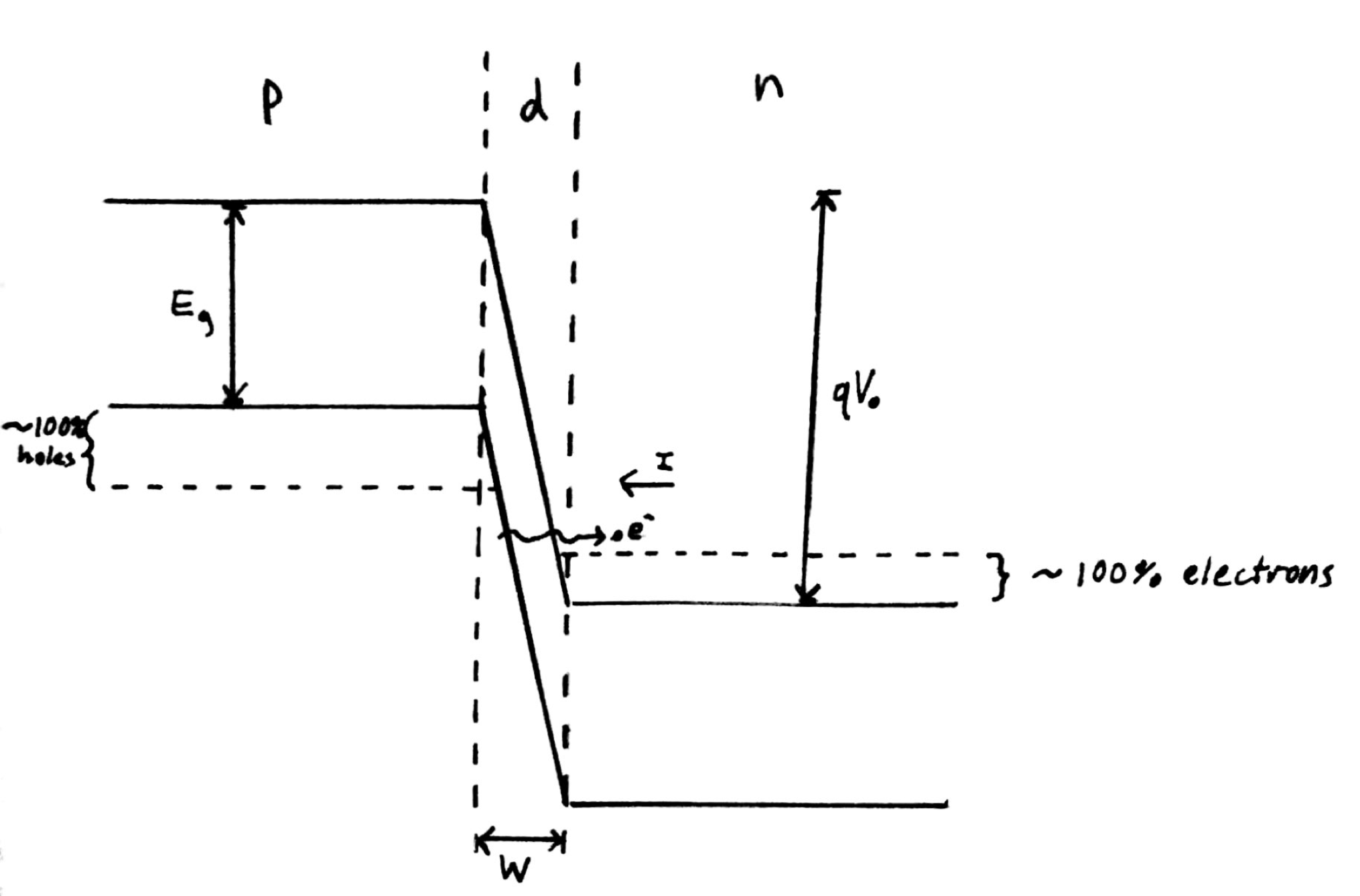 Fig. 1: Band diagram representing Esaki diode under tunneling condition. The diode is reverse biased, allowing an electron on the p side to tunnel across to an empty state on the n side.
1-Dimensional Quantum Model
The Esaki diode’s potential barrier looks different from the barriers we’ve examined in class, in that it actually comprises two energy functions. Counterintuitive as this is, the important aspects of the barrier are its width, approximately W, and its finite height, qV0. Thus, since the “sides” of the barrier are nearly vertical when highly doped, we’ll approximate it as a simple rectangular barrier with the same dimensions. The potential on either side can simply be 0.
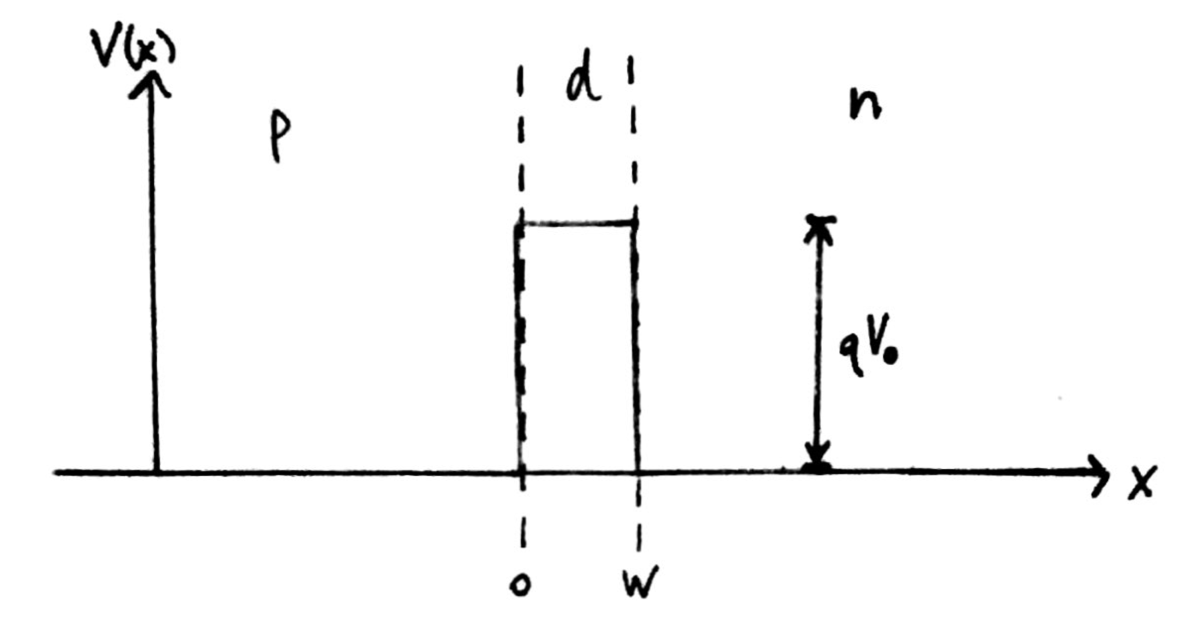 Fig. 2: Rectangular potential barrier representing Esaki diode barrier. This model has the same height and width as the real barrier.
An electron in this system has a wavefunction that satisfies the time-independent Schrödinger equation:
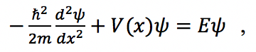
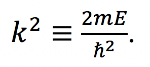
where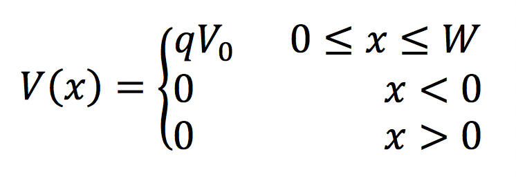
For the p and n regions, we can use the standard free particle solutions, assuming the electron is incident from the left:
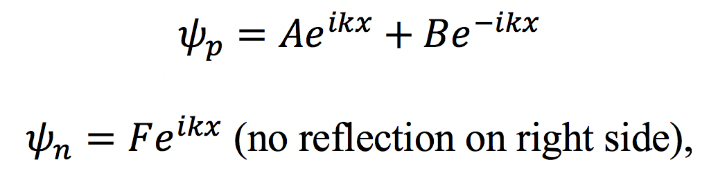
with
 .
.
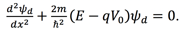
The depletion region’s TISE can be written as
.
So the solution is given by
![]()
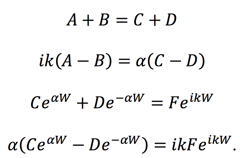
In order to determine the arbitrary coefficients, we must impose the boundary conditions, which state that the wavefunctions and their first derivatives must have continuity over each boundary. We get the following system of equations:
With some tedious algebra, we can solve for A in terms of F:
![]()
Now we can calculate the transmission coefficient:
![]()
Simplify and plug in original values for α and k to get expression in terms of given quantities:
![]()
This expression makes sense, because the limit as W goes to infinity is 0, and the limit as W goes to 0 is 1, meaning the electron is only likely to tunnel for small W. Note also that as the contact potential V0 goes to infinity, T goes to 0, as we would expect from an infinite potential well. Initially, we assumed the electron was incident from the p-side, as in the reverse bias case, but the mirror symmetry of our model means that as far as the barrier is concerned, we can expect identical behavior for an electron incident from the n-side.
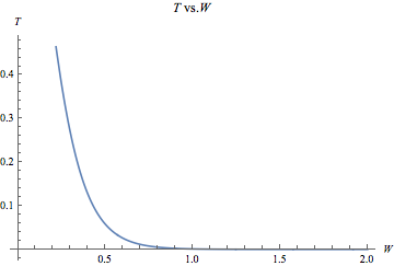 Fig. 3: This graph was produced in Mathematica using rough estimates for the energy values in the T equation. The numbers on the axes are not intended to represent actual quantities, and the graph merely suggests the shape of the function.
Conclusion
Although this model is very much an oversimplification of what the potential barrier in an Esaki diode actually looks like, it demonstrates the sort of behavior we would expect from the real thing, namely the behavior of the transmission coefficient with respect to the extremes of barrier width. Although the key characteristics of the tunnel diode are dependent on the doping of the two semiconductor materials, which falls outside the scope of this course, the rectangular barrier model focuses purely on the quantum mechanical process that lies at the core of this diode’s function.
Sources
Goswami, Amit. (1997). Quantum Mechanics. (2nd ed.). Waveland Press, Inc.
Griffiths, David J. (2004). Introduction to Quantum Mechanics (2nd ed.). Prentice Hall.
Streetman, Ben G., Banerjee, Sanjay Kumar. (1988). Solid State Electronic Devices (7th ed.). Pearson.
