This page was written by Alexandra Bello ’12
Optical Chitin
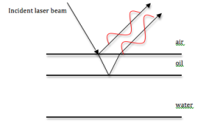
The term iridescence is used to describe the filtering of light due to thin film interference. Many thin films occur in nature. Beetles’ shells are essentially multiple thin films layered on top of each other. By directing a light beam at a beetle’s shell, the interference of the light can be studied and structural information about the beetle can be obtained.
Physical Mechanism: Thin film interference occurs when an incident beam of light is reflected by both the top and bottom of a film. As part of the beam is reflected off the bottom of the film, the period of the light shifts. This creates constructive or destructive interference between light reflected from each surface. The difference in refractive indices between the film, air and other materials the beam may pass through also alter the phase shift of the light.

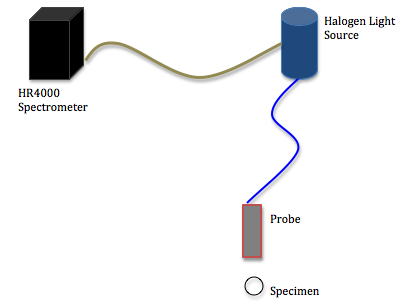
About the Spectrometer:
The spectrometer being used is an Ocean Optics High-Resolution 4000 spectrometer. A halogen light source shines light down a fiber-optic cable to the end of a probe, which is positioned toward a specimen. The reflected light bounces off the object and travels back up the cable and into the spectrometer where the reflected light is processed. The wavelengths of any light that is reflected is then graphed on a computer using the program SpectraSuite.
May 24-28, 2010
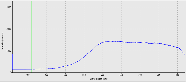
This week, preliminary light spectra of the sample beetles were taken. Each specimen was placed under a reflection spectrometer with a halogen light source and a graph was generated. Many of the beetles showed a spectrum with a high intensity at green wavelengths.

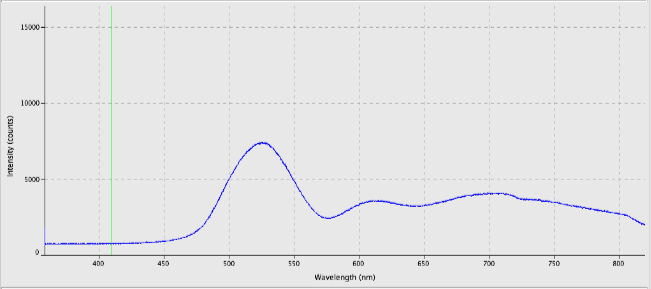
Other beetles iridesced at red or yellow wavelengths.

May 31- June 4, 2010
At this time, a mathematical model is necessary to analyze spectral data. The software Matlab will be used to model the light reflection off a single thin film with known thickness and index of refraction.
Matrix Methods
Matrix methods can be used to model this problem. A system of equations can be turned into matrices. In this case, a translation matrix can be created that is specific to an individual thin film. Multiple translation matrices can be added as well, to model multiple thin films.


Modeling Thin Films
The equation
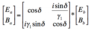
relates the characteristics of the film to the incident light. The terms Ea and Ebdescribe the electric field and the terms Ba and Bbdescribe the magnetic field of the incident light.
The matrix
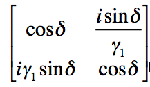
can be used to describe the film where
![]()
![]()
The variable n is the refractive index of the film, t is the thickness, λ is the wavelength of the incident light and
![]()
is the inverse of the speed of light in air.
For this project, all incident light is near normal so the cosθ terms become 1. The δ (phase difference) and γ terms can be specified for unique films. For a single film, this 2×2 matrix is called the transfer matrix, M. For multiple films, individual 2×2 matrices are multiplied together to create the transfer matrix of a system. The elements of the M matrix are then used in this equation to find the reflection coefficient of the system:
![]()
The γ terms are found by the same equation used earlier, but the n values are the refractive indices of the surrounding material (in this case air) and the substrate. The reflection coefficient is related to R, the reflectance of the system, by the equation:
![]()
By plotting wavelength vs. R, a graph can be generated that clearly shows areas of constructive and destructive interference in the spectrum. This graph will be useful in predicting the spectra that may be observed from certain species of beetle. Currently, a Matlab program is being written.
Pedrotti, Frank L., Leno S. Pedrotti, and Leno Matthew. Pedrotti. “Matrix Methods in Paraxial Optics.” Introduction to Optics. 3rd ed. N.J.: Pearson Prentice Hall, 2007. 406-07.
June 7-11, 2010
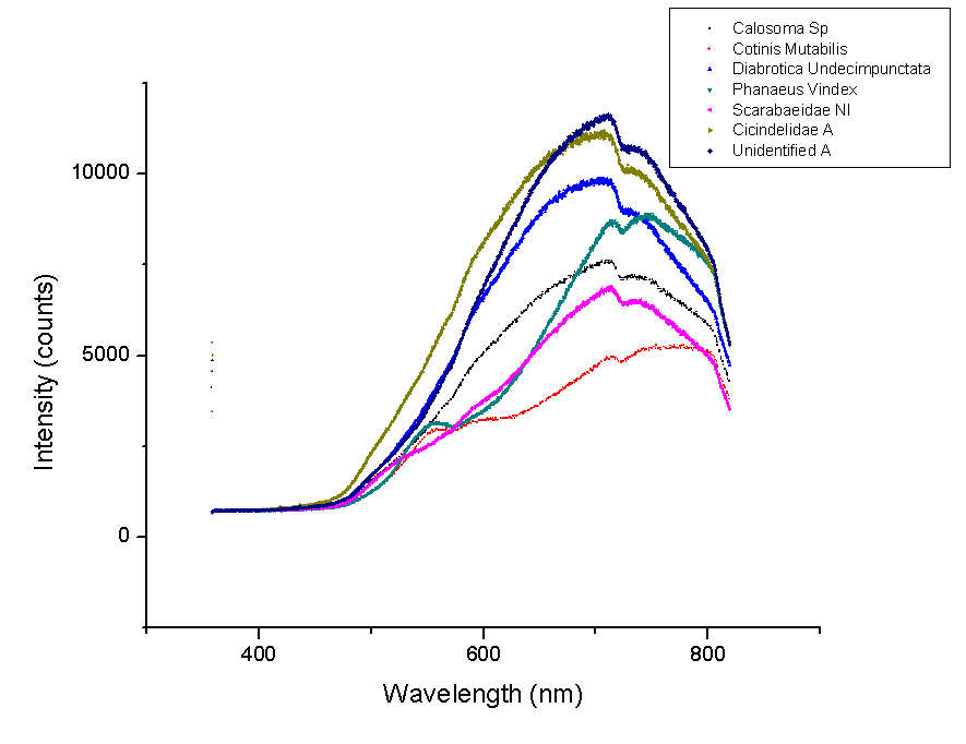
This week, plots of the spectra were generated using Origin. The y-axis is measured in counts of intensity measured by the spectrometer and the x-axis is the wavelength of those counts in nm. Each different color represents a different species of beetle and the letters NI mean the species is not identified yet. The spectra were taken from the left portion of each beetle’s back section. These plots compare beetles in the same family.
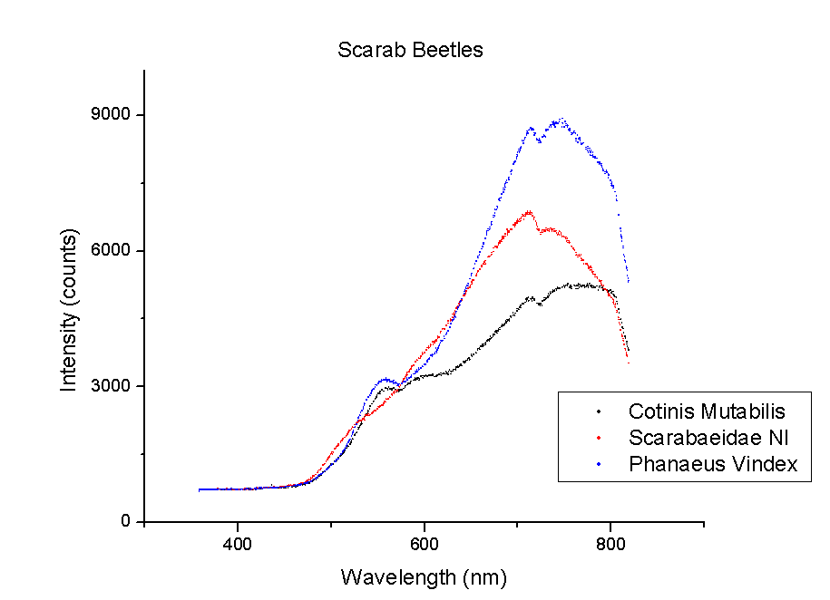
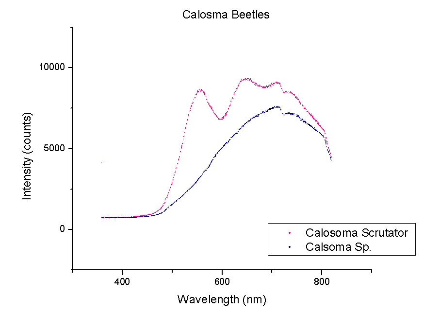
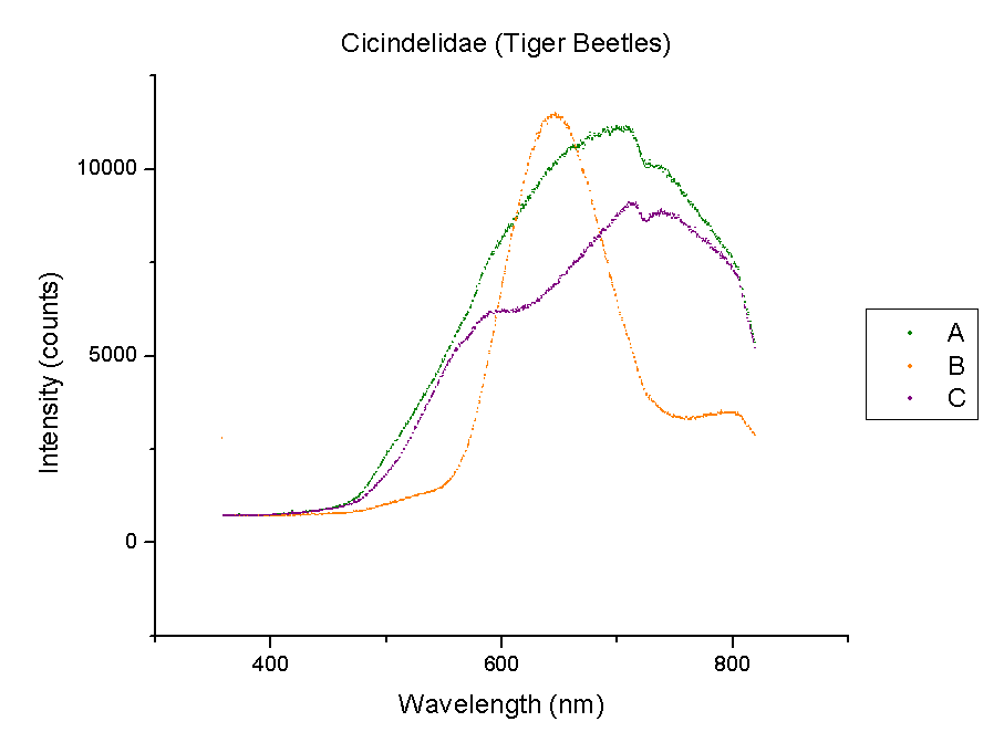
It should be noted that a notch at 725 nm is present in every spectra. This could mean a certain element or pigment is present in all these beetles. It could also be created by the experimental set-up. Whether this is due to a structural trait shared by all beetles or is caused by the spectrometer itself is unclear. In order to rule out error from the machine, more spectra must be taken of materials that are very different from beetle shells.
June 14-18. 2010
After finding the 725 nm notch, more spectral data was taken from objects in the lab. These objects included clothes, desktops, books and human skin. Spectra of a “stink bug” (nazara viridula) and several various flies were also taken. The notch appeared on all the spectral graphs. This means it is probably attributed to the spectrometer and not an outside source. This notch will provide an obstacle for mathematical modeling because it will need to be accounted for.
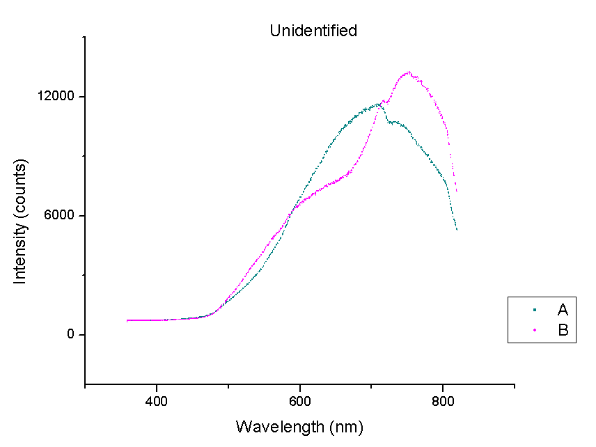
This week new graphs were made. Below is a comparison of beetles with similarly shaped spectra. These beetles will most likely have layered structures of similar number of layers, indices of refraction or both.
These spectra have the largest peak between 600 and 800 nm. It is likely that they have the same number of layers as well as layers with indices of refraction that are similar.
June 21-25, 2010
This week, the reflectance of a single thin film with known index of refraction placed over a glass substrate was graphed using Matlab. This code can be changed according to the index of refraction of the film and the reflectance can be re-plotted.

Each color represents a film with a different index of refraction.
blue- n=2; red- n=1.8; yellow- n=1.6; cerulean- n=1.4; green- n=1.2; magenta- n=1. Notice the instance of total destructive interference when path difference/wavelength is equal to 0.5.
Calibrating the Spectrometer
The spectrometer being used is calibrated to record diffuse reflections. It needs to record specular reflections. Diffuse reflection occurs when light enters a material and scatters off the particles inside of it. This creates multiple rays of light that reflect and refract throughout the material. When these rays exit the material, they propagate in different directions. 
During diffuse reflection in colored objects, certain wavelengths of light are absorbed by the particles and only the wavelengths of the object’s color are emitted. In specular reflection, light reflects off the surface of the object and does not interact with the particles. Light from a single incoming direction is reflected in a single outgoing direction. It obeys the Law of Reflection, meaning the angle of incidence is equal to the angle of reflection.

Objects made from non-absorbing powder, fibers or polycrystalline material make good diffusers of light. This includes plaster, paper and marble. Snow also diffuses light very well. Polished metals make nearly perfect specular reflectors. The metals in mirrors such as aluminum and silver are good examples. Many objects reflect light both specularly and diffusely.It is most common for objects to have between 5% and 10% specular reflection. In these cases, only the diffuse light can be colored. Wavelengths of light reflected specularly are all reflected at the same intensity, creating white light. Iridescence, however, is created by specularly reflected light but is colored, due to the phase shift and consequent interference of the light waves.
Kerker, M. (1909). The Scattering of Light. New York: Academic.
In beetles, color due to pigmentation is made visible by diffuse reflection while the color caused by iridescence is visible due to specular reflection, making a specular reflection spectra useful.
June 28-July 2, 2010
This week we travel to Delaware State University. Our goal is to learn how to perform Laser Induced Breakdown Spectroscopy (LIBS), and to test as many samples as we can. During LIBS, a high power infrared laser is used to turn a sample into a plasma. Fiber-optic cables then record the spectra of all the components of that sample. For more information, please see the LIBS page on the Vassar Applied Optics Laboratory blog homepage.
We brought with us quantum dots on silicon wafers that were made by Prof. Jenny Magnes. Because the wafers are stored in methanol, we spend the better part of the week trying to completely remove the methanol from the wafers using ultrasound. This technique keeps breaking the wafers but the pieces are still large enough to take data with.
July 5-9, 2010
This week, I move on to learn how to use a confocal microscope. I will use this to examine cross-sections of beetle shells and look at the structure and any fluorescence in the shells.
Fluorescence occurs when a substance that has absorbed light or other electromagnetic radiation emits light at a different wavelength. If a material fluoresces at a certain wavelength under the influence of a certain type of light, it can give clues to the structure and composition of the material. If a material fluoresces a wavelength closer to the red end of the spectrum than the incident laser light, then the light decreases in frequency and energy when it interacts with the material. If the sample fluoresces closer to the blue end of the spectrum, the light increases in frequency and energy.
A confocal microscope uses a laser to illuminate a small point on the sample and a pinhole in a optical plane to detect fluorescence and eliminate out of focus signal. Because only fluorescence close to the optical plane is detected, the resolution of the image created is much better than in a standard wide-field fluorescent microscope.
The microscope used at Delaware State is called a Leica SP5 and has four different lasers: a 405 nm diode, an argon and two HeNe lasers. This makes it possible to illuminate the sample with wavelengths throughout the visible spectrum, allowing the researcher to observe different kinds of fluorescence. It uses a software called Leica to generate images of the samples and shows the fluorescence of the sample at different parts of the visible spectra when illuminated by different wavelengths of light.
Samples were prepared by cutting small sections from the right wing and underside of the beetles. Samples from the wings were labeled as “b” and samples from the bottom shell were labeled “c.” As many of the beetles have ridges along the wings, these samples were cut in two different ways: parallel and perpendicular to the ridges. In addition, each beetle was given a number from 1 through 13. Each sample was placed, standing on it’s edge, on a glass slide with double sided tape.

This photo is an overlay of all the fluorescence observed with this sample. As is evident, the sample emits light mostly in the green and yellow portion of the spectrum, which is expected. However, parts of the sample fluoresce at the blue end of the spectrum. This is surprising because, as of now, I don’t know a mechanism that would increase the frequency of light emitted by a beetle shell.

Many beetles did not fluoresce in some parts of the shell. In this beetle, none of the inner layers fluoresce.
July 12-16, 2010
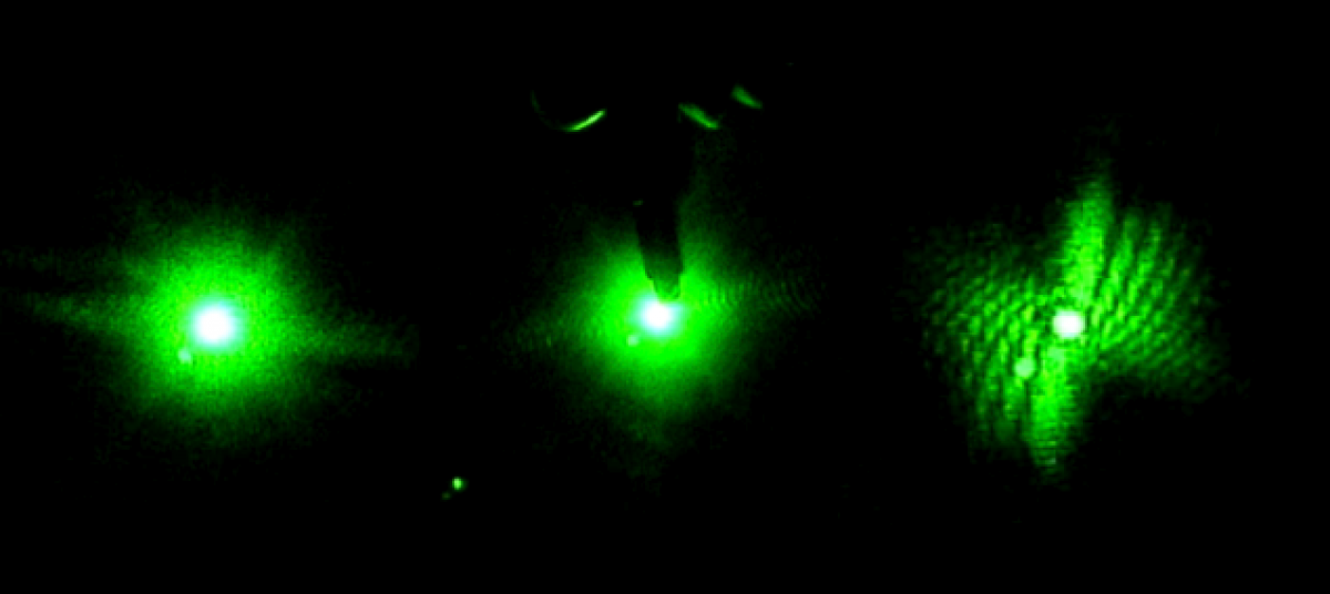
This week we were able to photograph quantum dots with the confocal microscope. These are the same dots that we brought to test using LIBS. We took cross sections of the wafers as well as pictures of the wafers lying flat.

The thin pink line is the side of the wafer that contains the quantum dots. The dark parts to the right are just a shadow of the wafer and to the left is the wafer itself. At the right and left edges of the picture, the tape used to mount the silicon fluoresces, but this is not the quantum dots.

This cross section is harder to see because neither edge of the wafer fluoresces. However, the thick black spot in the center is the wafer itself and the fluorescent spots on the left and right sides are the tape. While the cross sectionalphotographs are difficult to glean information from, the pictures taken of the flat wafers proved more useful.


The untreated silicon has very few marks on the surface. It does not fluoresce perfectly evenly but it is obvious that the entire surface is homogeneous.

The darker area consists of quantum dots or wells. The thick black line on the left is the edge of the wafer. As we zoom in, we can see the wells in greater detail.

These dark spots are images of single quantum wells. Quantum dot’s are made by exposing hydrofluoric acid on a silicon wafer to laser light. It is unclear why the acid does not eat away the silicon evenly, but rather produces individual wells. The samples photographed above were left at Delaware State College to be studied using LIBS at a later time.
July 19-23, 2010
After arriving back at our laboratory at Vassar, I spoke with Prof. Joe Tanksi in the Chemistry department about looking for a crystalline structure in the beetle shells. It is sometimes possible for chitin to form crystals, but it is not known if beetle shells are crystalline. After observing the samples I brought back from Delaware under a microscope, Prof. Tanski told me that he can perform x-ray crystallography on them if I grind them into a powder.

The samples were then placed in an x-ray spectrometer. If the shells had a crystal structure, we would have seen a diffraction pattern that indicated a repetitive pattern of atoms within the shell. This is would most likely be a set of rings that are spaced regularly apart. Instead, we saw one thick ring that indicated layers were present with a separation of 5 Å. This was unexpected, as we had believed beetle shell layers to be crystalline. However, it is likely that the layers have a regularity similar to the regularity of atoms in a crystal structure. The 5 Å spacing will need to be investigated further because this is not large enough to produce interference of light in the visible spectrum, which have observed previously.
Thank you to our collaborators:
Varada Iruvanti, Adjunct Professor in Physics, Vassar College
and Robert Suter, Professor in Biology
This page is maintained by Alexandra Bello. Class of 2012.
looking good!